
This week Intel held its annual Architecture Day event for select press and partners. As with previous iterations, the company disclosed details about its next generation architectures set to come to the market over the next twelve months. Intel has promised the release of its next-generation consumer and mobile processor family, Alder Lake, to come by the end of the year and today the company is sharing a good number of details about the holistic design of the chips as well as some good detail about the microarchitectures that form this hybrid design: Golden Cove and Gracemont. Here is our analysis of Intel’s disclosure.
Alder Lake: Intel 12th Gen Core
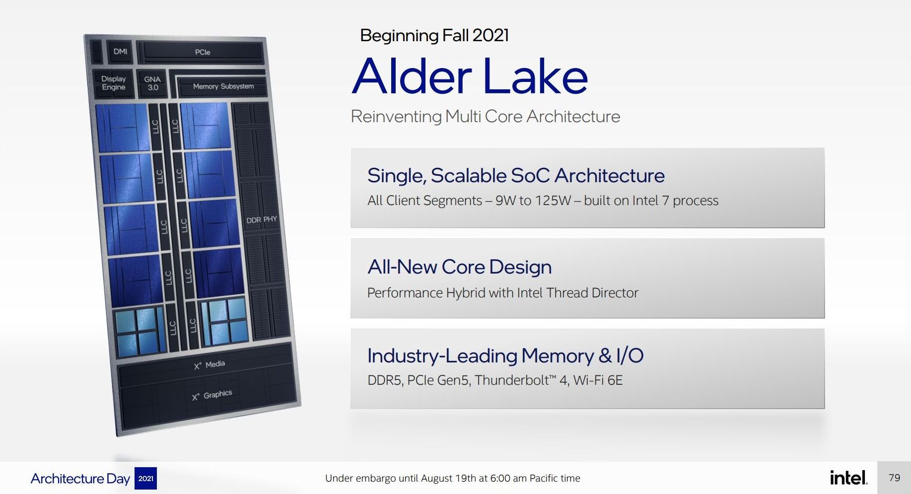
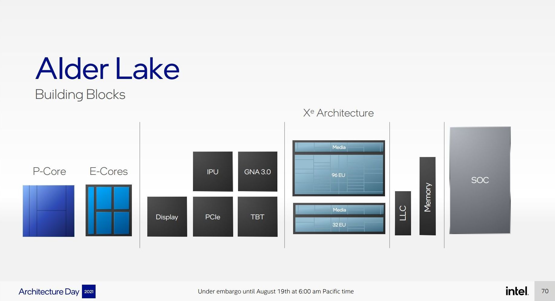
As mentioned in previous announcements, Intel will launch its Alder Lake family of processors into both desktop and mobile platforms under the name of Intel’s 12th Gen Core Processors with Hybrid Technology later this year. This is Intel’s second generation hybrid architecture built on Intel 7 process node technology. The hybrid design follows Intel Lakefield designs for small notebooks launched last year. The nature of a hybrid design in Intel nomenclature involves having a series of high ‘Performance’ cores paired with a number of high ‘Efficiency’ cores. Intel has simplified this into P-core and E-core terminology.
For Alder Lake, the processor designs feature Performance cores based on a new Golden Cove microarchitecture, and Efficiency cores based on a new Gracemont architecture. We will cover both over the course of this article, however the idea is that the P-core is preferential for single threaded tasks that require low latency, and the E-core is better in power limited or multi-threaded scenarios. Each Alder Lake SoC will physically contain both, however Intel has not yet disclosed the end-user product configurations.
Each of the P-cores has the potential to offer multithreading, whereas the E-cores are one thread per core. This means there will be three physical designs based on Alder Lake:
- 8 P-core + 8 E-core (8C8c/24T) for desktop on a new LGA1700 socket
- 6 P-core + 8 E-core (6C8c/20T) for mobile UP3 designs
- 2 P-core + 8 E-core (2C8c/12T) for mobile UP4 designs
Intel typically highlights UP4 mobile designs for very low power installs, down to 9 W, whereas UP3 can cover anything from 12 W to 35 W (or perhaps higher), but when asked about the power budgets for these processors, Intel stated that more detail will follow when product announcements are made. Intel did confirm that the highest client power, presumably on the desktop processor, will be 125 W.
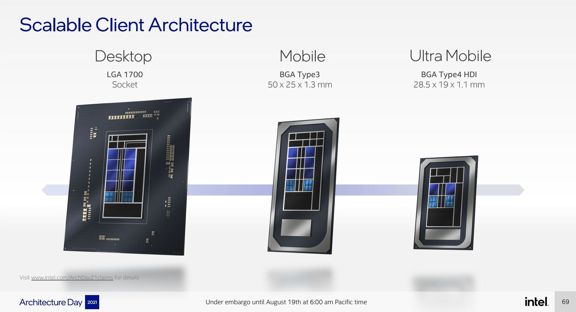
Highlighted in our discussions is how modular Intel has made Alder Lake. From a range of base component options, the company mixed and matched what it felt were the best combination of parts for each market.
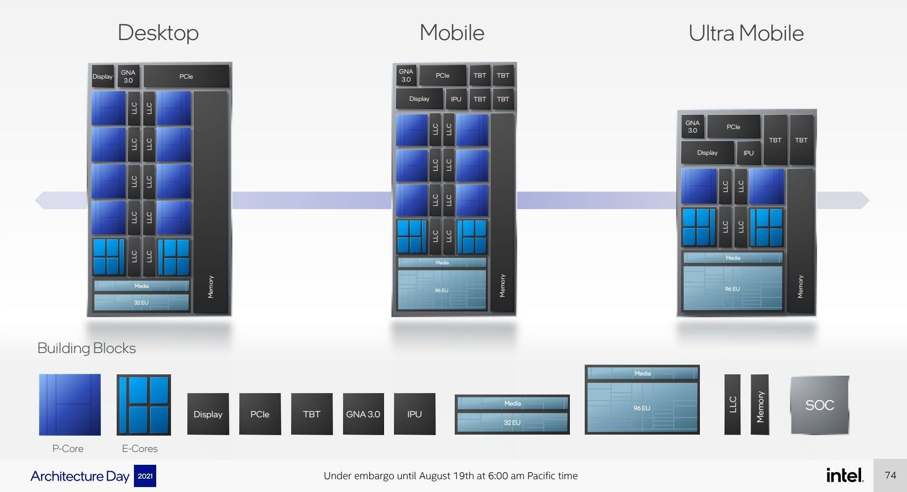
Here it shows that four E-cores takes up the same physical space as one P-core, but also that the desktop hardware will at most have 32 EUs (Execution Units) for Xe-LP graphics (same as the previous generation), while both of the mobile processors will offer 96 physical EUs that may be disabled down based on the specific line item in the product stack.
All three processors will feature Intel’s next generation Gaussian Neural Accelerator (GNA 3.0) for minor low power AI tasks, a display engine, and some level of PCIe, however the desktop processor will have more. Only the mobile processors will get an Image Processing Unit (IPU), and Thunderbolt 4 (TBT), and here the big UP3 mobile processor gets four ports of Thunderbolt whereas the smaller UP4 will only get two. The desktop processor will not have any native Thunderbolt connectivity.
A bit more info on the Desktop Processor IO and Interconnect
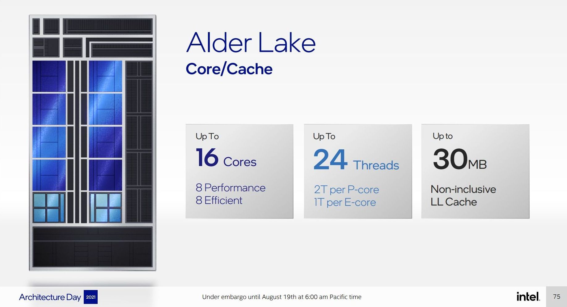
We’ll cover a bit more detail about the core designs later in this article, but Intel did showcase some of the information on the desktop processor. It confirmed explicitly that there would be 16 total cores and 24 threads, with up to 30 MB of non-inclusive last level/L3 cache.
In contrast to previous iterations of Intel’s processors, the desktop processor will support all modern standards: DDR5 at 4800 MT/s, DDR4-3200, LPDDR5-5200, and LPDDR4X-4266. Alongside this the processor will enable dynamic voltage-frequency scaling (aka turbo) and offer enhanced overclocking support. What exactly that last element means we’re unclear of at this point.
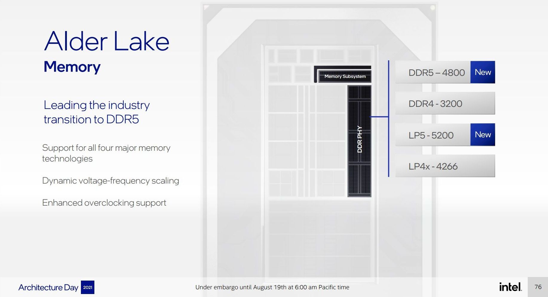
Intel confirmed that there will not be separate core designs with different memory support – all desktop processors will have a memory controller that can do all four standards. What this means is that we may see motherboards with built-in LPDDR5 or LPDDR4X rather than memory slots if a vendor wants to use LP memory, mostly likely in integrated small form factor designs but I wouldn’t put it past someone like ASRock to offer a mini-ITX board with built in LPDDR5. It was not disclosed what memory architectures the mobile processors will support, although we do expect almost identical support.
On the PCIe side of things, Alder Lake’s desktop processor will be supporting 20 lanes of PCIe, and this is split between PCIe 4.0 and PCIe 5.0.
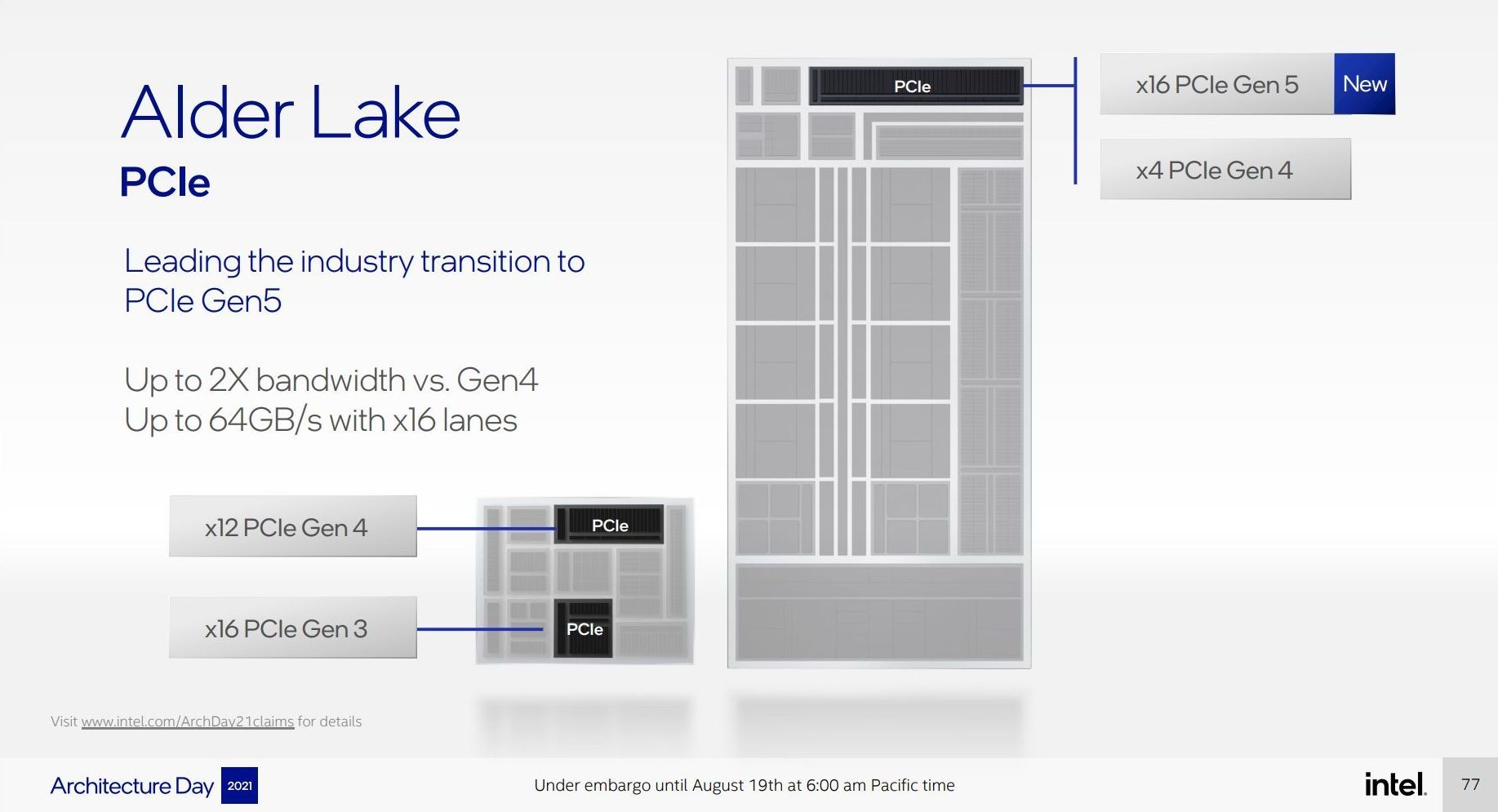
The desktop processor will have sixteen lanes of PCIe 5.0, which we expect to be split as x16 for graphics or as x8 for graphics and x4/x4 for storage. This will enable a full 64 GB/s bandwidth. Above and beyond this are another four PCIe 4.0 lanes for more storage. As PCIe 5.0 NVMe drives come to market, users may have to decide if they want the full PCIe 5.0 to the discrete graphics card or not
Intel also let it be known that the top chipset for Alder Lake on desktop now supports 12 lanes of PCIe 4.0 and 16 lanes of PCIe 3.0. This will allow for additional PCIe 4.0 devices to use the chipset, reducing the number of lanes needed for items like 10 gigabit Ethernet controllers or anything a bit spicier. If you ever thought your RGB controller could use more bandwidth, Intel is only happy to provide.
Intel did not disclose the bandwidth connectivity between the CPU and the chipset, though we believe this to be at least PCIe 4.0 x4 equivalent, if not higher.
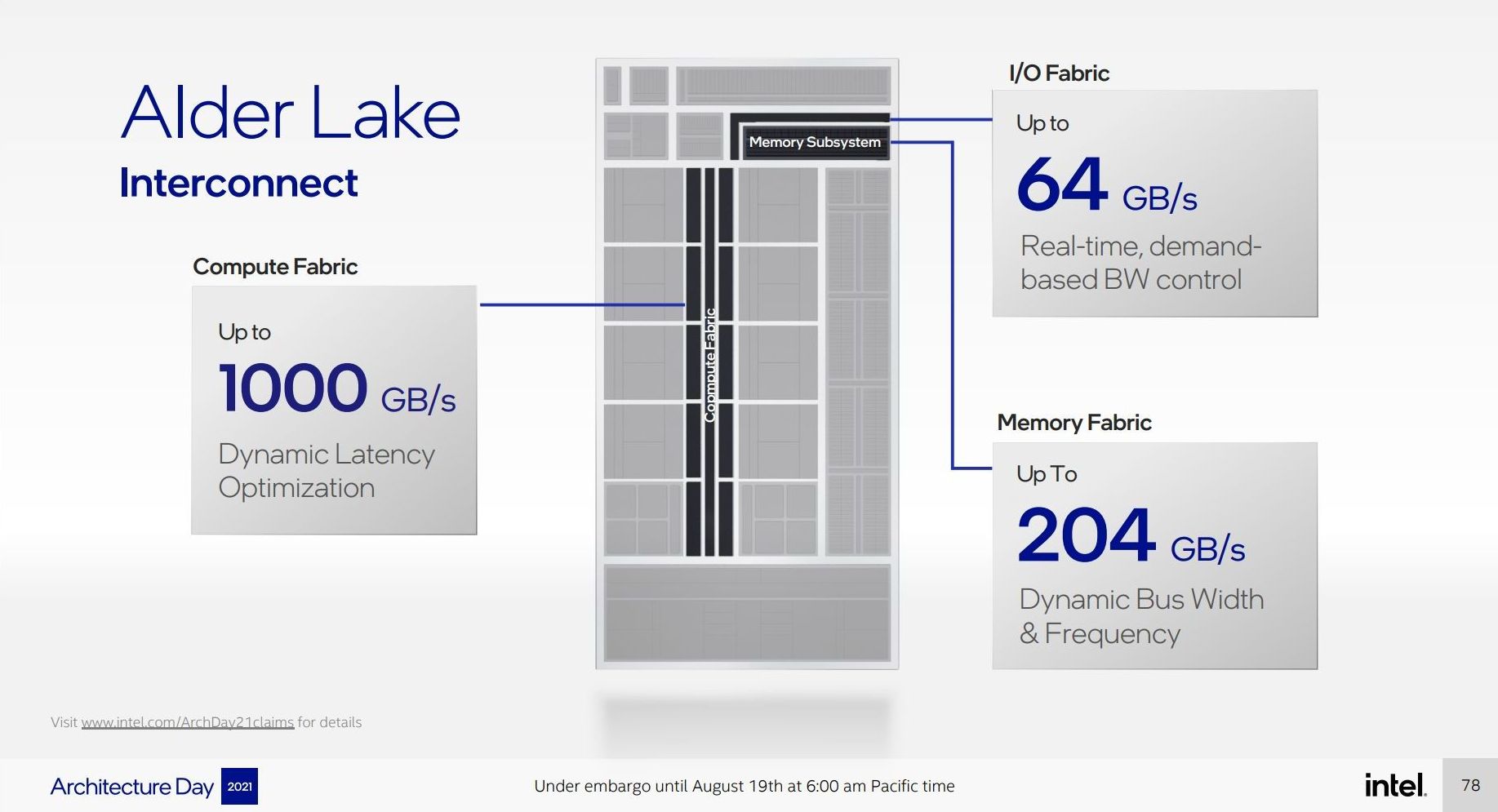
The Alder Lake processor retains the dual-bandwidth ring we saw implemented in Tiger Lake, enabling 1000 GB/s of bandwidth. We learned from asking Intel in our Q&A that this ring is fully enabled regardless of whether the P-cores or E-cores are being used – Intel can disable one of the two rings when less bandwidth is needed, which would save power, however based on previous testing this single ring could end up drawing substantial power compared to the E-cores in low power operation. (This may be true in the mobile processors as well, which would have knock on effects for mobile battery life.)
The 64 GB/s of IO fabric is in line with the PCIe 5.0 x16 numbers we saw above, however the 204 GB/s of memory fabric bandwidth is a confusing number. Alder Lake features a 128-bit memory bus, which allows for 4x 32-bit DDR5 channels (DDR5 has two 32-bit channels per module, so 2 modules still), however in order to reach 204 GB/s in that configuration requires DDR5-12750; Intel has rated the processor only at DDR5-4800, less than half that, so it is unclear where this 204 GB/s number comes from. For perspective, Intel’s Ice Lake does 204.8 GB/s, and that’s a high-power server platform with 8 channels of DDR4-3200.
This final slide mentions TB4 and Wi-Fi 6E, however as with previous desktop processors, these are derived from controllers attached to the chipset, and not in the silicon itself. The mobile processors will have TBT integrated, but the desktop processor does not.
This slide also mentions Intel Thread Director, which we want to address on the next page before we get to the microarchitecture analysis.
One of the biggest criticisms that I’ve levelled at the feet of Intel since it started talking about its hybrid processor architecture designs has been the ability to manage threads in an intelligent way. When you have two cores of different performance and efficiency points, either the processor or the operating system has to be cognizant of what goes where to get the best result from the end-user. This requires doing additional analysis on what is going on with each thread, especially new work that has never been before.
To date, most desktop operating systems operate on the assumption that all cores and the performance of everything in the system is equal. This changed slightly with simultaneous multithreading (SMT, or in Intel speak, HyperThreading), because now the system had double the threads, and these threads offered anywhere from zero to an extra 100% performance based on the workload. Schedulers were hacked a bit to identify primary and secondary threads on a core and schedule new work on separate cores. In mobile situations, the concept of an Energy Aware Scheduler (EAS) would look at the workload characteristics of a thread and based on the battery life/settings, try and schedule a workload where it made sense, particularly if it was a latency sensitive workload.
Mobile processors with Arm architecture designs have been tackling this topic for over a decade. Modern mobile processors now have three types of core inside – a super high performance core, regular high performance cores, and efficiency cores, normally in a 1+3+4 or 2+4+4 configuration. Each set of cores has its own optimal window for performance and power, and so it relies on the scheduler to absorb as much information as possible to determine the best way to do things.
Such an arrangement is rare in the desktop space - but now with Alder Lake, Intel has an SoC that has SMT performance cores and non-SMT efficient cores. With Alder Lake it gets a bit more complex, and the company has built a technology called Thread Director.
That’s Intel Thread Director. Not Intel Threat Detector, which is what I keep calling it all day, or Intel Threadripper, which I have also heard. Intel will use the acronym ITD or ITDT (Intel Thread Director Technology) in its marketing. Not to be confused with TDT, Intel’s Threat Detection Technology, of course.
Intel Threadripper Thread Director Technology
This new technology is a combined hardware/software solution that Intel has engineered with Microsoft focused on Windows 11. It all boils down to having the right functionality to help the operating system make decisions about where to put threads that require low latency vs threads that require high efficiency but are not time critical.
First you need a software scheduler that knows what it is doing. Intel stated that it has worked extensively with Microsoft to get what they want into Windows 11, and that Microsoft have gone above and beyond what Intel needed. This fundamental change is one reason why Windows 11 exists.
So it’s easy enough (now) to tell an operating system that different types of cores exist. Each one can have a respective performance and efficiency rating, and the operating system can migrate threads around as required. However the difference between Windows 10 and Windows 11 is how much information is available to the scheduler about what is running.
In previous versions of Windows, the scheduler had to rely on analysing the programs on its own, inferring performance requirements of a thread but with no real underlying understanding of what was happening. Windows 11 leverages new technology to understand different performance modes, instruction sets, and it also gets hints about which threads rate higher and which ones are worth demoting if a higher priority thread needs the performance.
Intel classifies the performance levels on Alder Lake in the following order:
- One thread per core on P-cores
- Only thread on E-cores
- SMT threads on P-cores
That means the system will load up one thread per P-core and all the E-cores before moving to the hyperthreads on the P-cores.
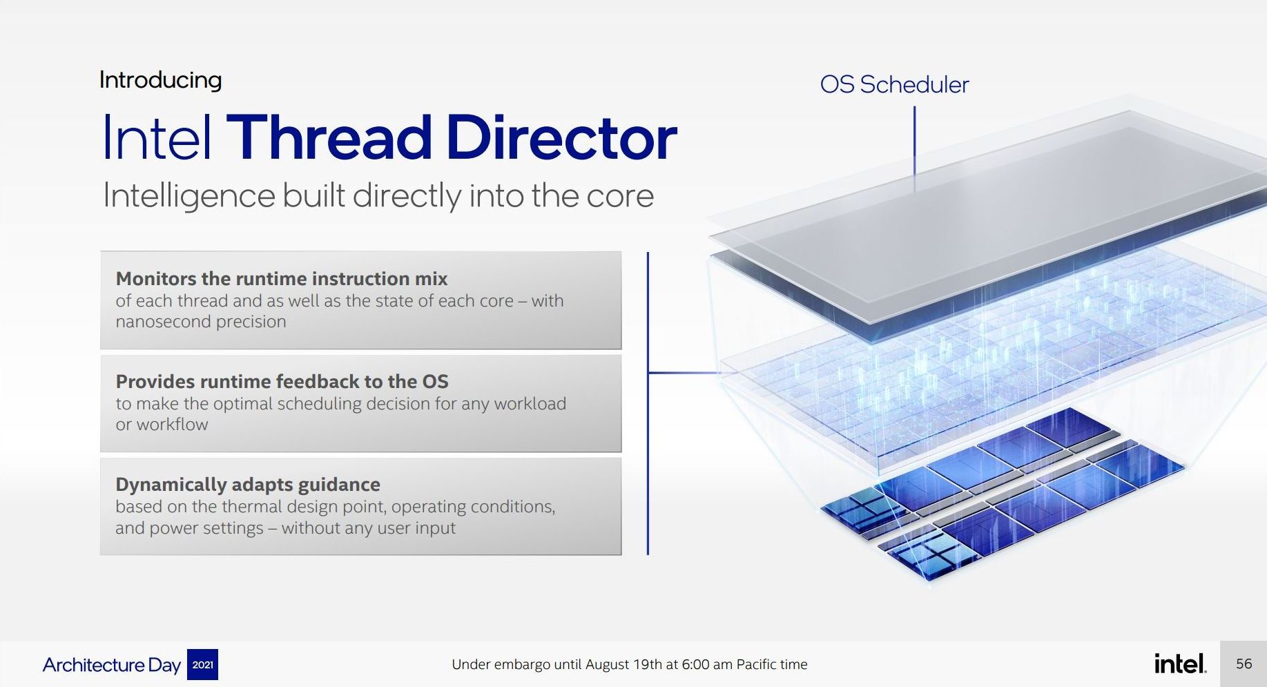
Intel’s Thread Director controller puts an embedded microcontroller inside the processor such that it can monitor what each thread is doing and what it needs out of its performance metrics. It will look at the ratio of loads, stores, branches, average memory access times, patterns, and types of instructions. It then provides suggested hints back to the Windows 11 OS scheduler about what the thread is doing, whether it is important or not, and it is up to the OS scheduler to combine that with other information about the system as to where that thread should go. Ultimately the OS is both topologically aware and now workload aware to a much higher degree.
Inside the microcontroller as part of Thread Director, it monitors which instructions are power hungry, such as AVX-VNNI (for machine learning) or other AVX2 commands that often draw high power, and put a big flag on those for the OS for prioritization. It also looks at other threads in the system and if a thread needs to be demoted, either due to not having enough free P-cores or for power/thermal reasons, it will give hints to the OS as to which thread is best to move. Intel states that it can profile a thread in as little as 30 microseconds, whereas a traditional OS scheduler may take 100s of milliseconds to make the same conclusion (or the wrong one).
On top of this, Intel says that Thread Director can also optimize for frequency. If a thread is limited in a way other than frequency, it can detect this and reduce frequency, voltage, and power. This will help the mobile processors, and when asked Intel stated that it can change frequency now in microseconds rather than milliseconds.
We asked Intel about where an initial thread will go before the scheduling kicks in. I was told that a thread will initially get scheduled on a P-core unless they are full, then it goes to an E-core until the scheduler determines what the thread needs, then the OS can be guided to upgrade the thread. In power limited scenarios, such as being on battery, a thread may start on the E-core anyway even if the P-cores are free.
For users looking for more information about Thread Director on a technical, I suggest reading this document and going to page 185, reading about EHFI – Enhanced Hardware Frequency Interface. It outlines the different classes of performance as part of the hardware part of Thread Director.
It’s important to understand that for the desktop processor with 8 P-cores and 8 E-cores, if there was a 16-thread workload then it will be scheduled across all 8 P-cores with 8 threads, then all 8 E-cores with the other 8 threads. This affords more performance than enabling the hyperthreads on the P-cores, and so software that compares thread-to-thread loading (such as the latest 3DMark CPU Profile test) may be testing something different compared to processors without E-cores.
On the question of Linux, Intel only went as far to say that Windows 11 was the priority, and they’re working upstreaming a variety of features in the Linux kernel but it will take time. An Intel spokesperson said more details closer to product launch, however these things will take a while, perhaps months and years, to get to a state that could be feature-parity equivalent with Windows 11.
One of the biggest questions users will ask is about the difference in performance or battery between Windows 10 and Windows 11. Windows 10 does not get Thread Director, but relies on a more basic version of Intel’s Hardware Guided Scheduling (HGS). In our conversations with Intel, they were cagy to put any exact performance differential metrics between the two, however based on understanding of the technology, we should expect to see better frequency efficiency in Windows 11. Intel stated that even though the new technology in Windows 11 will mean threads will move more often than in Windows 10, potentially adding latency, in their testing it wasn’t in any way human perceivable. Ultimately because the Win11 configuration can also optimize for power and efficiency, especially in mobile, Intel puts the win on Windows 11.
The only question is if Windows 11 will launch in time for Alder Lake.
Within Alder Lake and Sapphire Rapids, we find Intel’s brand-new performance core (P-Core) microarchitecture, called Golden Cove. The new microarchitecture and core design follows the Willow Cove core in Tiger Lake, the Sunny Cove core in Ice Lake, and the derivative Cypress Cove core in Rocket Lake.
Although the new design is a follow-up over the last few years of core microarchitectures, Intel sees the Golden Gove as a major step-function update, with massive revamps of the fundamental building blocks of the CPU, going as far as calling it as allowing performance for the next decade of compute, meaning Intel is seemingly planning on using it as the basis for the evolution of cores for at least a few years.
The last time we had seen major upgrades to Intel’s core front-end was in Ice Lake, making notable increases in the microarchitecture’s out-of-order execution capabilities and depth, while Sunny Cove and Cypress Cove were more iterative designs focusing on the memory subsystem.
Golden Cove, in comparison, makes gigantic changes to the microarchitecture’s front-end – in fact, Intel states that this is the largest microarchitectural upgrade in the core family in a decade, mirroring similar changes in magnitude to what Skylake had done many years ago.
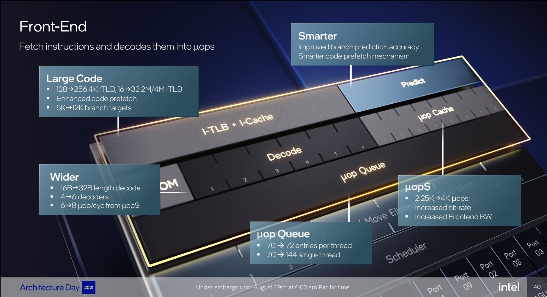
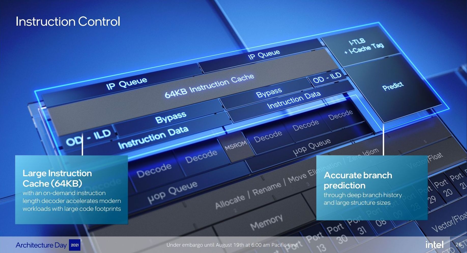
Starting off with the directly most obvious change: Intel is moving from being a 4-wide decode machine to being a 6-wide microarchitecture, a first amongst x86 designs, and a major design focus point. Over the last few years there had been a discussion point about decoder widths and the nature of x86’s variable length instruction set, making it difficult to design decoders that would go wider, compared to say a fixed instruction set ISA like Arm’s, where adding decoders is relatively easier to do. Notably last year AMD’s Mike Clarke had noted while it’s not a fundamental limitation, going for decoders larger than 4 instructions can create practical drawbacks, as the added complexity, and most importantly, added pipeline stages. For Golden Cove, Intel has decided to push forward with these changes, and a compromise that had to be made is that the design now adds an additional stage to the mispredict penalty of the microarchitecture, so the best-case would go up from 16 cycles to 17 cycles. We asked if there was still a kind of special-case decoder layout as in previous generations (such as the 1 complex + 3 simple decoder setup), however the company wouldn’t dwell deeper into the details at this point in time. To feed the decoder, the fetch bandwidth going into it has been doubled from 16 bytes per cycle to 32 bytes per cycle.
Intel states that the decoder is clock-gated 80% of the time, instead relying on the µOP cache. This has also seen extremely large changes this generation: first of all, the structure has now almost doubled from 2.25K entries to 4K entries, mimicking a similar large increase we had seen with the move from AMD’s Zen to Zen2, increasing the hit-rate and further avoiding going the route of the more costly decoders.
Although the I-cache has remained the same in terms of size at 32KB, Intel has improved latencies for larger code coverage by increasing the L1 iTLB from 128 entries to 256 entries (16 -> 32 for 2M/4M hugepages).
Because the general misprediction penalty has gone up this generation, Intel is very much counter-acting this by massively improving branch prediction accuracy. First of all, the L2 BTB (branch target buffer) has grown to well over double with the structure increased from 5K entries to 12K entries, making this by far the biggest in the industry that we’re aware of (Zen3: 6.5K, Cortex-A77+: 8K, Apple: ?). It is also said that the branch predictors themselves are now smarter, with their accuracy being improved, although these are always quite a bit secretive in terms of their designs so we didn’t have too many details divulged.
The decoders and the µOP cache feed a µOP queue – beyond he 50% larger decoder width, the µOP cache also now sees an increased bandwidth and able to emit 8 µOPs instead of 6. The µOP queue itself has seen a structural change, for single threads (only one SMT logical core is loaded), the structure can be aggregated and the usable depth has doubled from 70 entries to 144 entries, while for dual threads, has gone up slightly from 70 to 72 entries per thread.
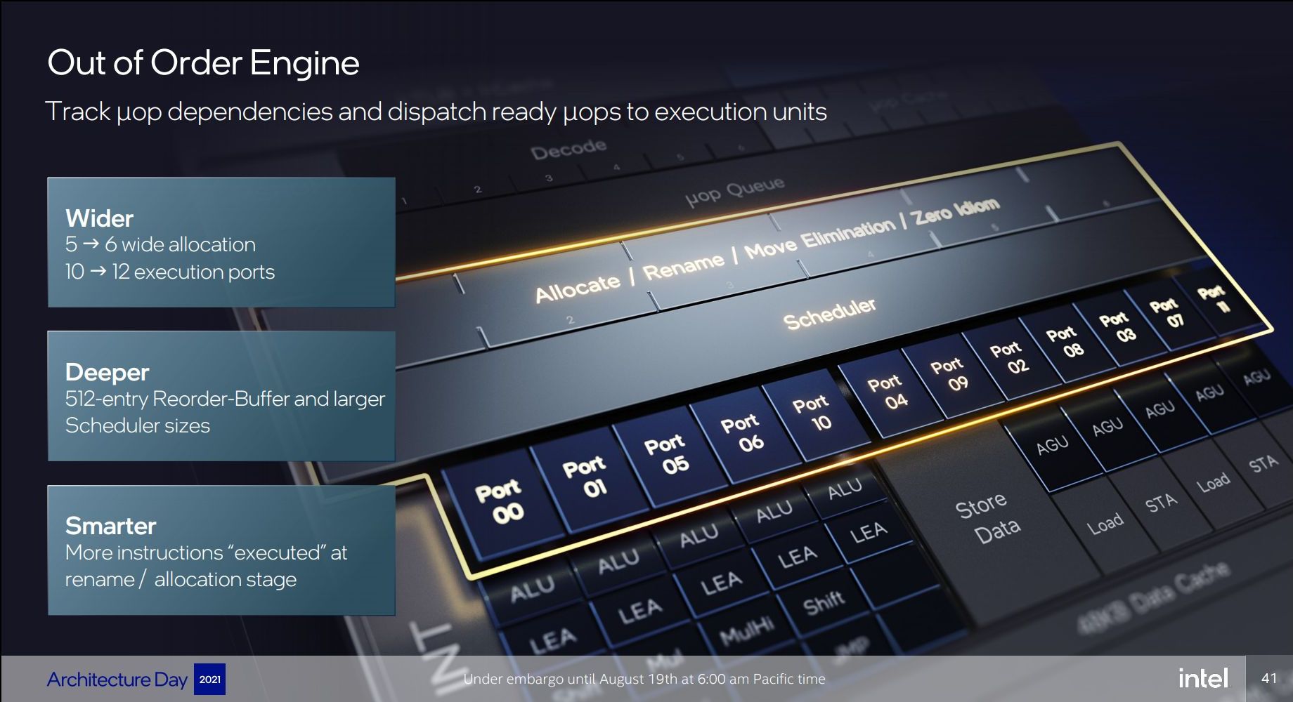
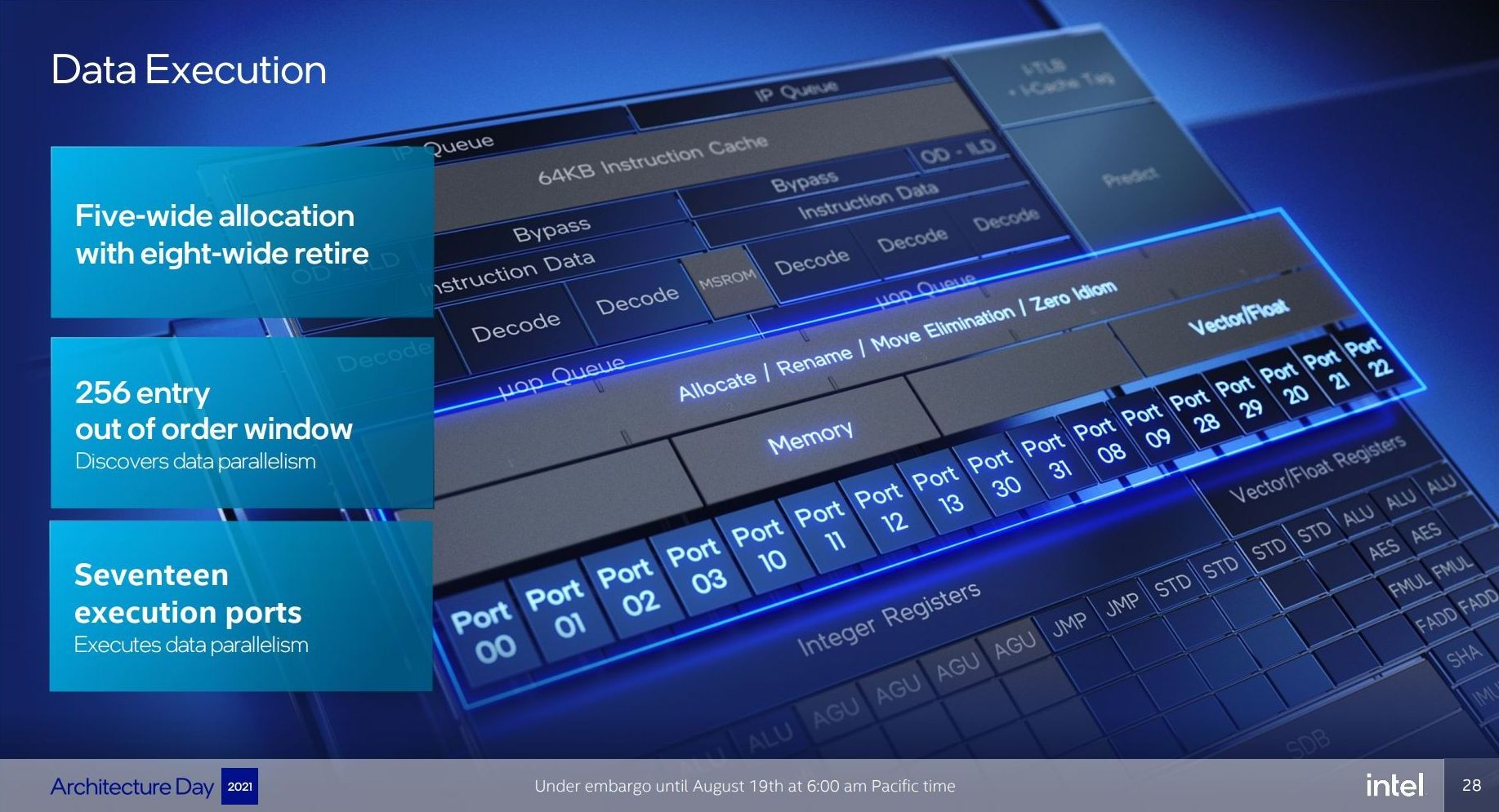
In the mid-core, there’s also been quite large changes. The core here increases from 5-wide to 6-wide, meaning that in theory it should still be a maximum 6 IPC with microarchitecture, though we’re talking about µOPs here and not actual instructions.
Intel is noting that they’re doing an increased amount of dependency resolution at the allocation stage, actually eliminating instructions that otherwise would have to actually emitted to the back-end execution resources. Intel here didn’t want to elaborate a lot, only stating that this capability has increased quite a lot generation over generation.
The out-of-order instruction window of Golden Cove is massively larger than Sunny Cove – increasing the re-order buffer (ROB) size from 352 to 512 entries. This is over double that of AMD’s Zen3 µarch, and really only second to Apple’s core microarchitecture which we’ve measured in at around 630 instructions. Traditionally, we’ve always been told that increasing the ROB has diminishing effects and always corelates with quite an increase in power consumption – but on the other hand we saw Apple achieve extremely high OOO-windows. It’s not clear how exactly Intel managed to increase their µarch by such a large degree in a single jump, but it’s a very impressive and admittedly unexpected design characteristic of the Golden Cove cores.
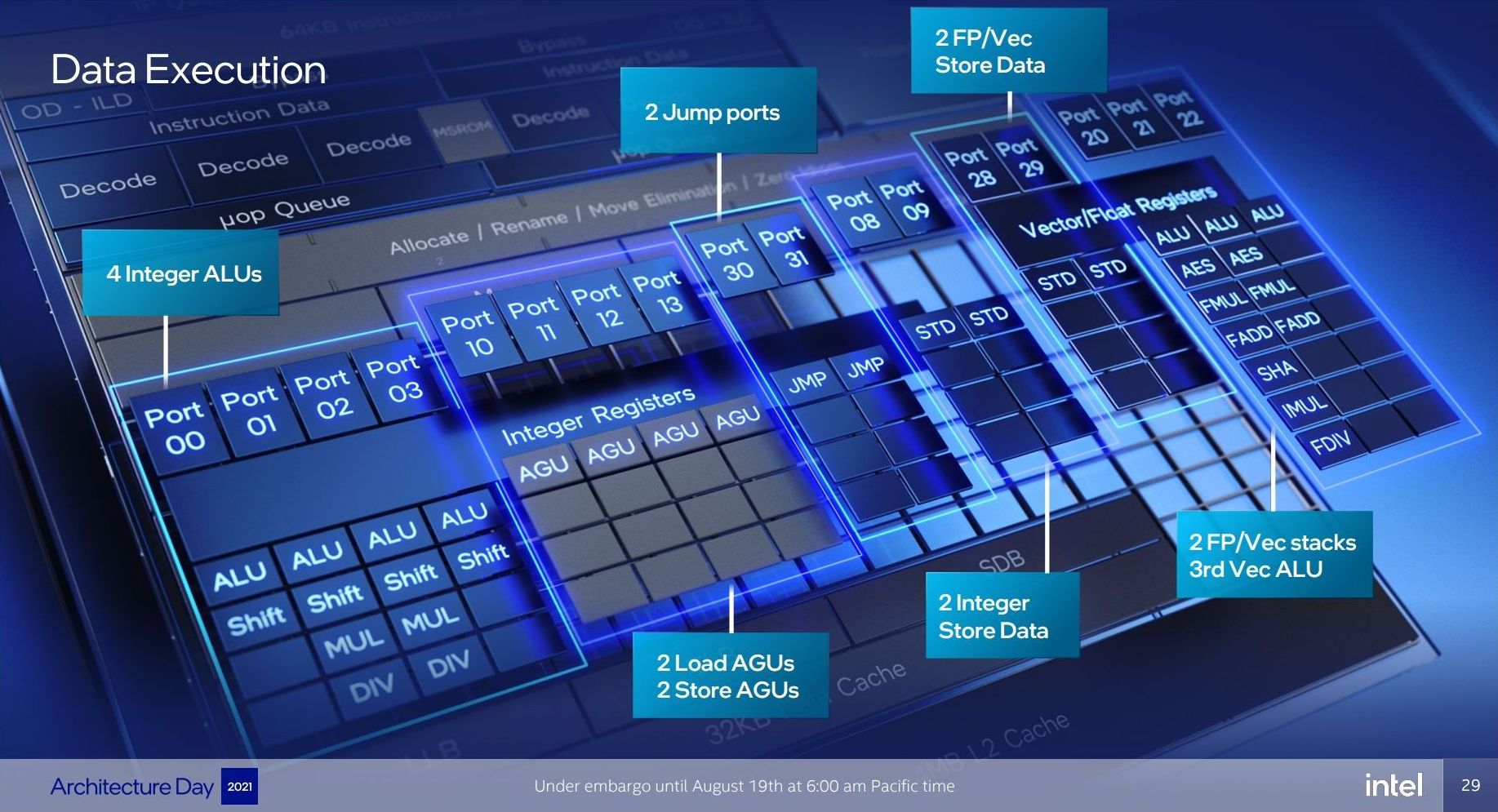
Moving onto the back-end, Intel has increased their execution width from 10 ports to 12 ports. Intel still continues to use merged execution port / reservation station design that characterises their cores in contrast to other µarchs from the competition, or even their own E-core microarchitectures, which use separate integer and FP/vector ports and pipelines.
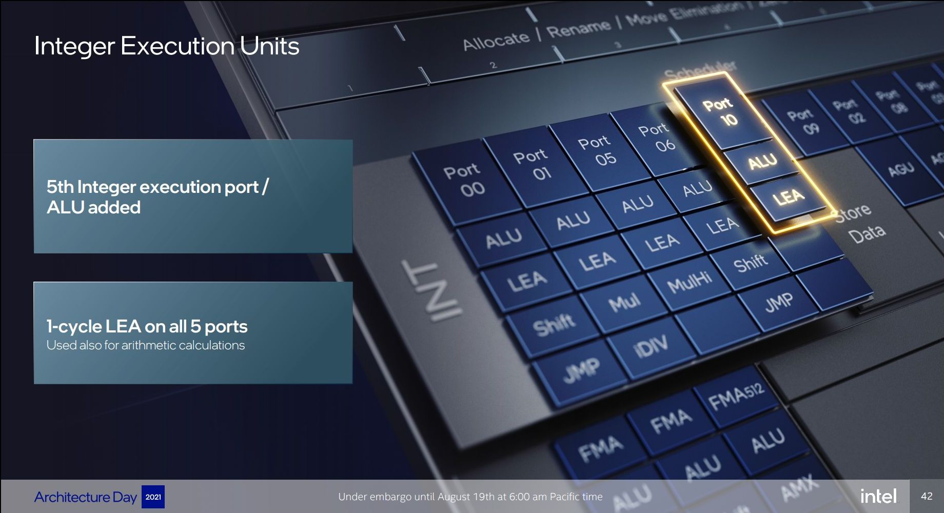
On the integer side of things, there’s now a fifth execution port and pipeline with simple ALU and LEA capabilities, which in theory makes this the widest x86 core in raw ALU throughput, although in mixed code the 5 pipelines are still somewhat comparatively narrower.
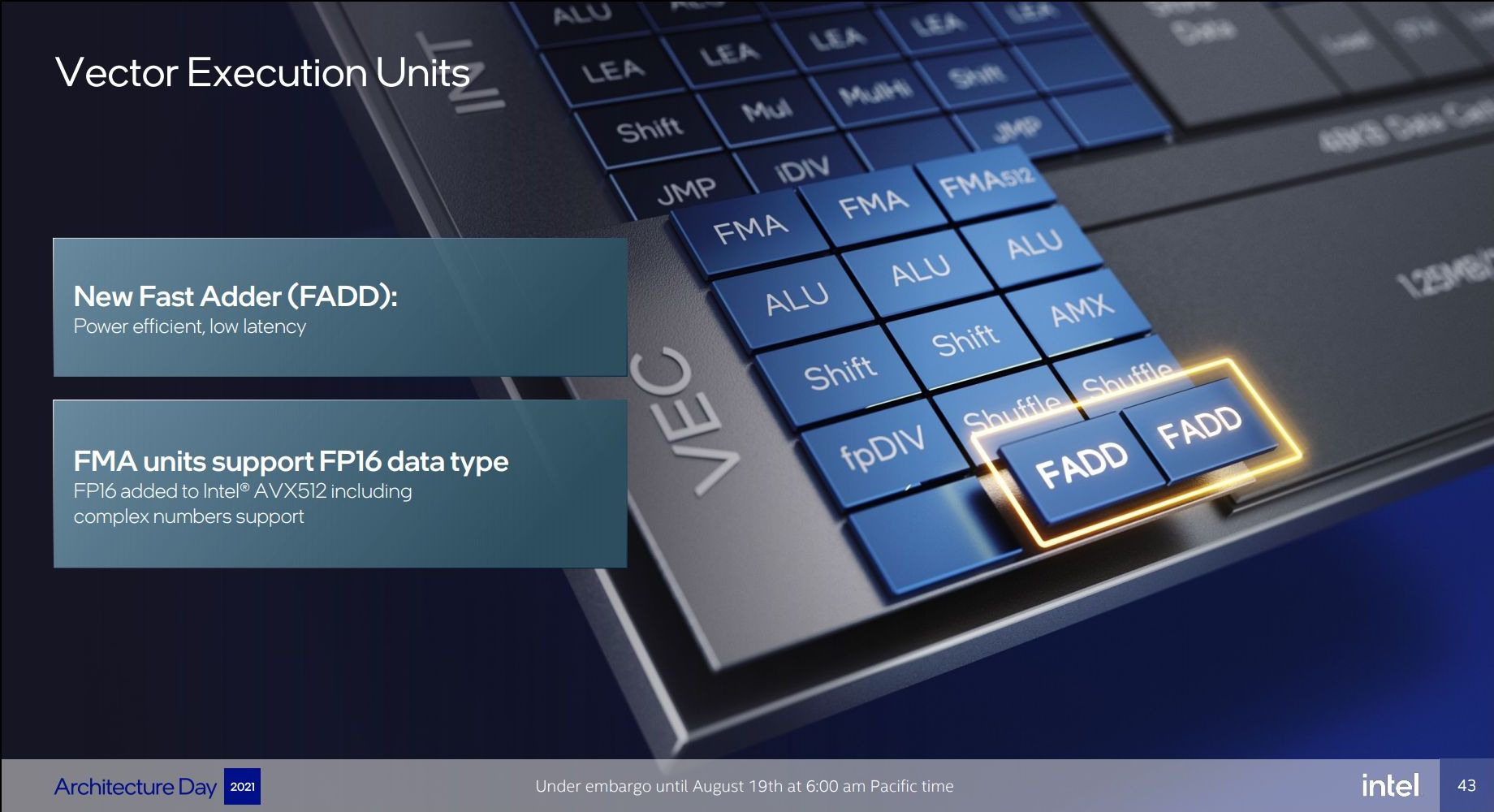
On the FP capabilities side of things, we’ve seen added dedicated FADD capabilities, which are far more efficient and lower latency than using the FMA units (when applicable). The FMA units now have also seen added support for FP16 data types, although this falls under the AVX512 umbrella consumer cores won’t see the capabilities.
In general, besides the added 5th ALU port/pipeline, the back-end execution resources of Golden Cove appear to be somewhat more conservative compared to the more substantial front-end changes of the core.
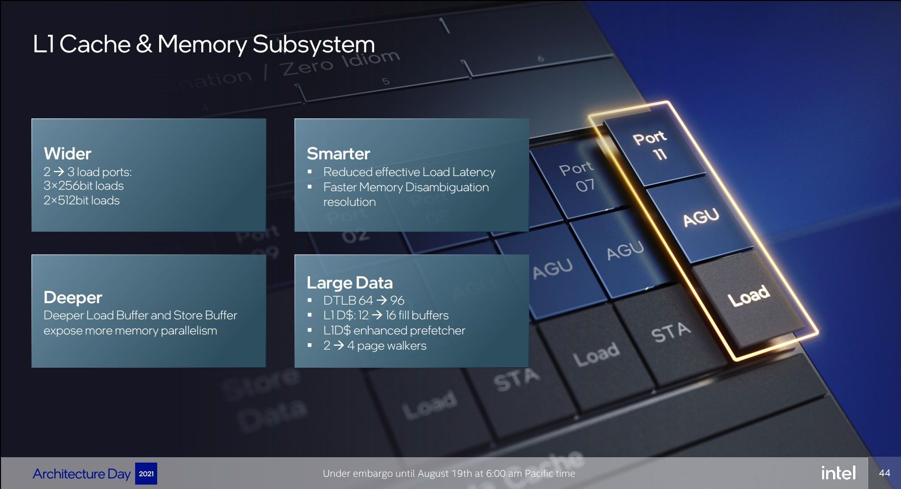
On the load & store front, we see the addition of an additional dedicated execution port with a load AGU, increasing the possible number of loads per cycle from 2 to 3, matching the upgrades we’ve seen from many other microarchitectures over the last few years.
For AVX512-enabled implementations of the µarch, it’s able to load up to 1KB/cycle from the L1, while consumer cores still see a 50% improvement for AVX2 256-bit loads with 3 per cycle.
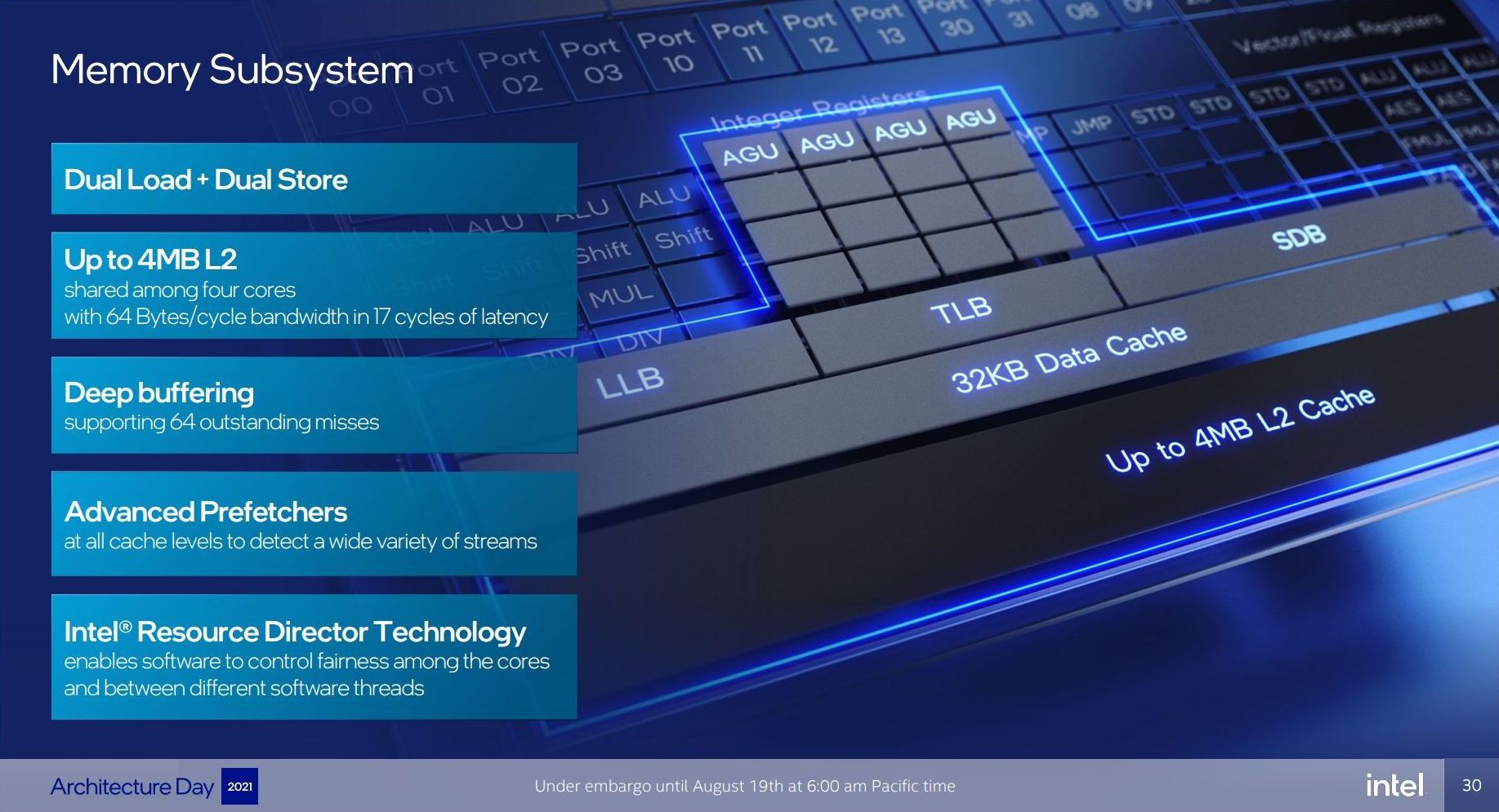
Intel, like many other, have noted that modern workloads have increased memory level parallelism, so they have increased the outstanding memory transactions from the core by increasing the L1D fill buffers from 12 to 16, and increasing the load and store buffers by undisclosed amounts. Similarly, to AMD, to better address sparse memory access workloads, the µarch has seen a doubling of page walkers from 2 to 4, able to look up pages in TLB misses.
The L1 DTLB has grown from 64 entries to 96 entries – Intel didn’t mention the L2 TLB which would mean it’s still at 2048 entries.
Intel has improved the prefetchers, nothing things such as “better stride prefetching in L1”, though beyond that the company hasn’t divulged much other details. We’ve seen a lot of advances in the industry in terms of prefetchers so it’ll be interesting to see how Golden Cove compared to the competition here.
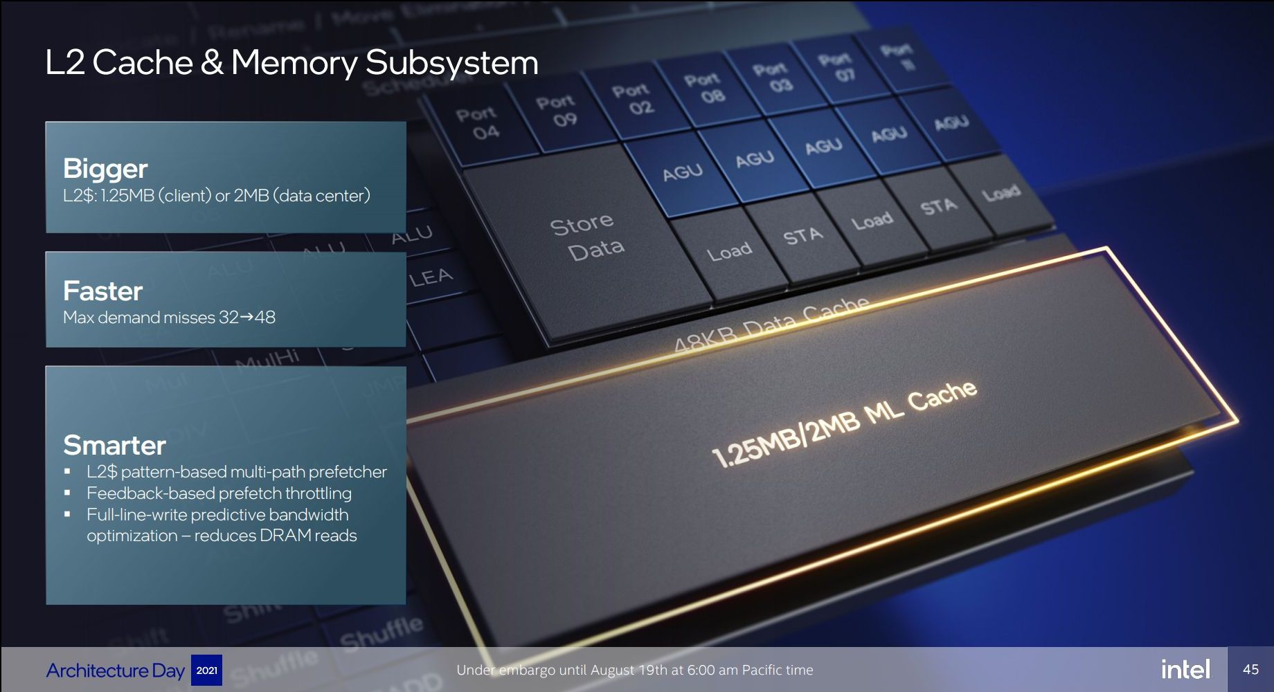
The L2 cache in Golden Cove remains at 1.25MB for consumer core variants, while the server variant grows it to 2MB compared to 1.25MB in the current Ice Lake-SP chips. Parallel data access outstanding requests for the memory subsystem has grown from 32 misses to 48, also further helping with increasing MLP capabilities of the core.
Intel also again notes there’s been prefetching improvements in the L2. What the company calls “full-line-write predictive bandwidth optimisation” is likely the same mechanism we saw in our review of Ice Lake-SP where the core can greatly improve bandwidth by avoiding RFO reads of cache lines that are going to be fully rewritten, which should greatly improve common generic operations such as memory copies.
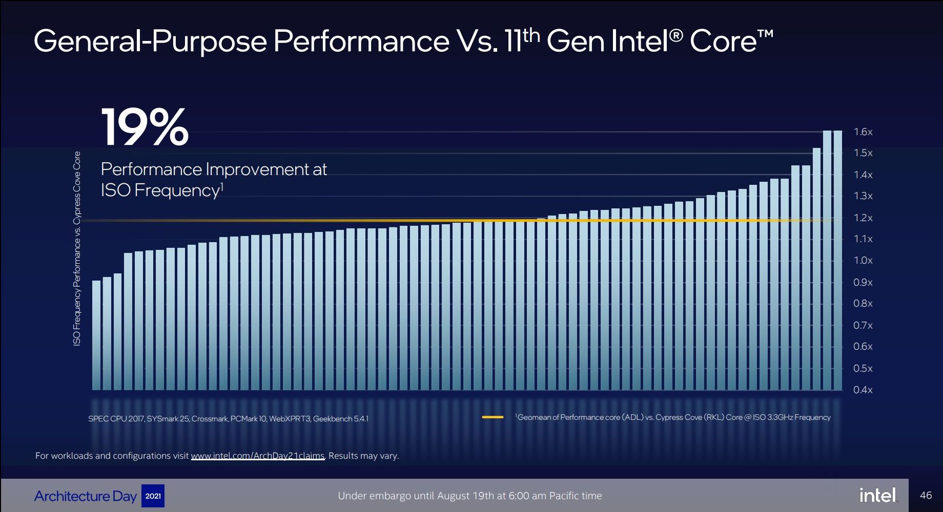
The aggregated changes of the new Golden Cove microarchitecture amount to a median IPC increase of 19% compared to Cypress Cove (Rocket Lake) - measured over a set of workloads including SPEC CPU 2017, SYSmark 25, Crossmark, PCMark 10, WebXPRT3, and Geekbench 5.4.1. We can see in the graph that there’s outlier workloads with up to +60% IPC, but also low outliers where the new design doesn’t improve thing much or even sees regressions, which is odd.
The front-end changes of Golden Cove indeed look like a major step-function: 50% wider decode, +25% wider µOP output and double the capacity, +45% deeper out-of-order execution buffer, massive branch prediction improvements. It’s possible that the more conservative back-end execution improvements overall lowered the end results.
19% IPC is still a very impressive figure, and one of Intel’s largest jumps in a decade, but the company is also comparing it to Cypress Cove, rather than their latest generation design, which is Willow Cove inside of the Tiger Lake chips. We would have wished for Intel to at least give us both comparisons, so that we would get an idea for both desktop as well as mobile improvements.
The smaller core as part of Intel’s hybrid Alder Lake design is called an E-core, and is built on the Gracemont microarchitecture. It forms part of Intel’s Atom family of processors, and is a significant microarchitectural jump over the previous Atom core design called Tremont.
- 2008: Bonnell
- 2011: Saltwell
- 2013: Silvermont
- 2015: Airmont
- 2016: Goldmont
- 2017: Goldmont Plus
- 2020: Tremont
- 2021: Gracemont
Based on Intel’s diagrams, the company is pitching that the size of its Golden Cove core means that in the space it would normally fit one of its P-core designs, it can enable a four core cluster of E-cores along with a shared 4MB L2 cache between them.
For performance, Intel has some pretty wild claims. It splits them up into single thread and multi-thread comparisons using SPECrate2017_int.
When comparing 1C1T of Gracemont against 1C1T of Skylake, Intel’s numbers suggest:
- +40% performance at iso-power (using a middling frequency)
- 40% less power at iso-performance (peak Skylake performance)
When comparing 4C4T of Gracemont against 2C4T of Skylake, Intel’s numbers suggest:
- +80% performance peak vs peak
- 80% less power at iso performance)peak Skylake performance
We pushed the two Intel slides together to show how they presented this data.
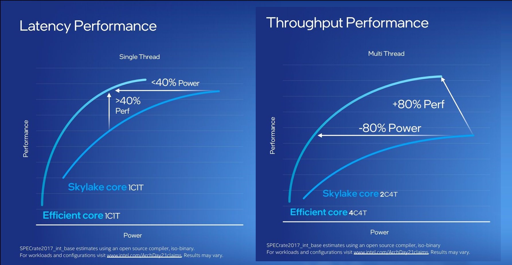
Is it just me, or is that ‘40% power’ on the ST graph on the left not 40% of the graph?
Anyway, by these graphics it looks like that for peak single thread, we should see around +8% better than Skylake performance while consuming just over half the power – look for Cinebench R20 scores for one Gracemont thread around 478 then (Skylake 6700K scored 443). With +8% for single thread in mind, the +80% in MT comparing 4 cores of Gracemont to two fully loaded Skylake cores seems a little low – we’ve got double the physical cores with Gracemont compared to Skylake here. But there’s likely some additional performance regression with the cache structure on the new Atom core, which we’ll get to later on this page.
These claims are substantial. Intel hasn’t compared the new Atom core generation on generation, because it felt that having AVX2 support would put the new Atom at a significant advantage. But what Intel is saying with these graphs is that we should expect better-than Skylake performance at much less power. We saw Skylake processors up to 28 cores in HEDT – it makes me wonder if Intel might not enable its new Atom core for that market. If that’s the case, where is our 64-core Atom version for HEDT? I’ll take one.
Front End
The big item about the Tremont front end of the core was the move to dual three-wide decode paths, enabling two concurrent streams of decode that could support 3 per cycle. That still remains in Gracemont, but is backed by a double-size 64 KB L1 Instruction cache. This ties into the branch predictor which enables prefetchers at all cache levels, along with a 5000-entry branch target cache which Intel says in improved over the previous generation.
Back on the decoder, Intel supports on-demand decode which stores a history of previous decodes in the instruction cache and if recent misses are recalled at the decode stage, the on-demand stream will pull directly from the instruction cache instead, saving time – if the prefetch/decode works, the content in the instruction cache is updated, however if it is doing poorly then the scope is ‘re-enabled for general fetches’ to get a better understanding of the instruction flow. This almost sounds like a micro-op cache without having a physical cache, but is more to do about instruction streaming. Either way, the decoders can push up to six uops into the second half of the front end.
For Gracemont, the reorder buffer size has increased from 208 in Tremont to 256, which is important aspect given that Gracemont now has a total of 17 (!) execution ports, compared to eight in Tremont. This is also significantly wider than the execution capabilities of Golden Cove's 12 ports, related to the disaggregated integer and FP/vector pipeline design. However, despite that width, the allocation stage feeding into the reservation stations can only process five instructions per cycle. On the return path, each core can retire eight instructions per cycle.
Back End
So it’s a bit insane to have 17 execution ports here. There are a lot of repeated units as well, which means that Gracemont is expecting to see repeated instruction use and requires the parallelism to do more per cycle and then perhaps sit idle waiting for the next instructions to come down the pipe. Overall we have
- 4 Integer ALUs (ALU/Shift), two of which can do MUL/DIV
- 4 Address Generator Units, 2 Load + 2 Store
- 2 Branch Ports
- 2 Extra Integer Store ports
- 2 Floating Point/Vector store ports
- 3 Floating Point/Vector ALUs: 3x ALUs, 2x AES/FMUL/FADD, 1x SHA/IMUL/FDIV
It will be interesting to see exactly how many of these can be accessed simultaneously. In previous core designs a lot of this functionality would be enabled though the same port – even Alder Lake’s P-core only has 12 execution ports, with some ports doing double duty on Vector and Integer workloads. In the P-core there is a single scheduler for both types of workloads, whereas in the E-core there are two separate schedulers, which is more akin to what we see on non-x86 core designs. It’s a tradeoff in complexity and ease-of-use.
The back-end is support by a 32 KiB L1-Data cache, which supports a 3-cycle pointer chasing latency and 64 outstanding cache misses. There are two load and two store ports, which means 2x16 byte loads and 2 x 16 byte stores to the L1-D.
There is also has a shared 4 MB L2 cache across all four E-cores in a cluster with 17-cycle latency. The shared L2 cache can support 64 bytes per cycle read/write per core, which Intel states is sufficient for all four cores. The new L2 supports up to 64 outstanding misses to the deeper memory subsystem – which seems fair, but has to be shared amongst the 4 cores.
Intel states that it has a Resource Director that will arbitrate cache accesses between the four cores in a cluster to ensure fairness, confirming that Intel are building these E-cores in for multi-threaded performance rather than latency sensitive scenarios where one thread might have priority.
Other Highlights
As the first Atom core to have AVX2 enabled, there are two vector ports that support FMUL and FADD (port 20 and port 21), which means that we should expect peak performance compared to previous Atoms to be substantial. The addition of VNNI-INT8 over the AVX unit means that Intel wants these E-cores to enable situations where high inference throughput is needed, such as perhaps video analysis.
Intel was keen to point out that Gracemont has all of its latest security features including Control Flow Enhancement Technology (CET), and virtualization redirects under its VT-rp feature.
Overall, Intel stated that the E-cores are tuned for voltage more than anything else (such as performance, area). This means that the E-cores are set to use a lot less power, which may help in mobile scenarios. But as mentioned before on the first page, it will depend on how much power the ring has to consume in that environment - it should be worth noting that each four core Atom cluster only has a single stop on the full ring in Alder Lake, which Intel says should not cause congestion but it is a possibility – if each core is fully loaded, there is only 512 KB of L2 cache per core before making the jump to main memory, which indicates that in a fully loaded scenario, that might be a bottleneck.
One of the big questions we should address here is how the P-cores and E-cores have been adapted to work inside a hybrid design. One of the critical aspects in a hybrid design is if both cores support different levels of instructions. It is possible to build a processor with an unbalanced instruction support, however that requires hardware to trap unsupported instructions and do core migration mid-execution. The simple way to get around this is to ensure that both types of cores have the same level of instruction support. This is what Intel has done in Alder Lake.
In order to get to this point, Intel had to cut down some of the features of its P-core, and improve some features on the E-core. The biggest thing that gets the cut is that Intel is losing AVX-512 support inside Alder Lake. When we say losing support, we mean that the AVX-512 is going to be physically fused off, so even if you ran the processor with the E-cores disabled at boot time, AVX-512 is still disabled.
Intel’s journey with AVX-512 has been long and fragmented. Some workloads can be vectorised – multiple bits of consecutive data all require the same operation, so you can pack them into a single register and perform it all at once with a single instruction. Designed as its third generation of vector instructions (AVX is 128-bit, AVX2 is 256-bit, AVX512 is 512-bit), AVX-512 was initially found on server processors, then mobile, and we found it in the previous version of desktop processors. At the time, Intel stated that by enabling AVX-512 on its processor line from top to bottom, it would encourage greater adoption, and they were leaning hard into this missive.
But that all changes with Alder Lake. Both desktop processors and mobile processors will now have AVX-512 disabled in all scenarios. But the silicon will still be physically present in the core, only because Intel uses the same core in its next generation server processors called Sapphire Rapids. One could argue that if the AVX-512 unit was removed from the desktop cores that they would be a lot smaller, however Intel has disagreed on this point in previous launches. What it means is that for the consumer parts we have some extra dark silicon in the design, which ultimately might help thermals, or absorb defects.
But it does mean that AVX-512 is probably dead for consumers.
Intel isn’t even supporting AVX-512 with a dual-issue AVX2 mode over multiple operations - it simply won’t work on Alder Lake. If AMD’s Zen 4 processors plan to support some form of AVX-512 as has been theorized, even as dual-issue AVX2 operations, we might be in some dystopian processor environment where AMD is the only consumer processor on the market to support AVX-512.
On the E-core side, Gracemont will be Intel’s first Atom processor to support AVX2. In testing with the previous generation Tremont Atom core, at 2.9 GHz it performed similarly to a Haswell 2.9 GHz Celeron processor, i.e. identical in non-AVX2 situations. By adding AVX2, plus fundamental performance increases, we’re told to expect ‘Skylake-like performance’ from the new E-cores. Intel also stated that both the P-core and E-core will be at ‘Haswell-level’ AVX2 support.
By enabling AVX2 on the E-cores, Intel is also integrating support for VNNI instructions for neural network calculations. In the past VNNI (and VNNI2) were built for AVX-512, however this time around Intel has done a version of AVX2-VNNI for both the P-core and E-core designs in Alder Lake. So while AVX-512 might be dead here, at least some of those AI acceleration features are carrying over, albeit in AVX2 form.
For the data center versions of these big cores, Intel does have AVX-512 support and new features for matrix extensions, which we will cover in that section.
Alder Lake is set to come to market for both desktop and mobile, and we’re expecting the desktop hardware to start to appear by the end of the year – perhaps a little latter for the rest of the family, but all-in-all we expect Intel is experiencing some serious squeaky bum time regarding to how all the pieces will fit in place at that launch. The two main critical factors are operating systems and memory.
Because Alder Lake is Intel’s first full-stack attempt to commercialize a hybrid design, it has had to work closely with Microsoft to enable all the features it needs to make managing a hybrid core design properly beneficial to users. Intel’s new Thread Director Technology couples an integrated microcontroller per P-core and a new API for Windows 11 such that the scheduler in the operating system can take hints about the workflow on the core at a super fine granularity – every 30 microseconds or so. With information about what each thread is doing (from heavy AVX2 down to spin lock idling), the OS can react when a new thread needs performance, and choose which threads need to be relegated down to the E-core or as a hyperthread (which is classified as slower than an E-core).
When I first learned Alder Lake was going to be a hybrid design, I was perhaps one of the most skeptical users about how it was going to work, especially with some of the limits of Windows 10. At this point today however, with the explanations I have from Intel, I’m more confident than not that they’ve done it right. Some side off-the-record conversations I have had have only bolstered the idea that Microsoft has done everything Intel has asked, and users will need Windows 11 to get that benefit. Windows 10 still has some Hardware Guided Scheduling, but it’s akin to only knowing half the story. The only question is whether Windows 11 will be fully ready by the time Alder Lake comes to market.
For memory, as a core design, Alder Lake will have support for DDR4 and DDR5, however only one can be used at any given time. Systems will have to be designed for one or the other – Intel will state that by offering both, OEMs will have the opportunity to use the right memory at the right time for the right cost, however the push to full DDR5 would simplify the platform a lot more. We’re starting to see DDR5 come to the consumer market, but not in any volume that makes any consumer sense – market research firms expect the market to be 10% DDR5 by the end of 2022, which means that consumers might have to be stay with DDR4 for a while, and vendors will have to choose whether to bundle DDR5 with their systems. Either way, there’s no easy answer to the question ‘what memory should I use with Alder Lake’.
Through The Cores and The Atoms
From a design perspective, both the P-core and E-core are showcasing substantial improvements to their designs compared to previous generations.
The new Golden Cove core has upgraded the front-end decoder, which has been a sticking point for analysis of previous Cove and Lake cores. The exact details of how they operate are still being kept under wraps, but having a 6-wide variable length decoder is going to be an interesting talking point against 8-wide fixed length decoders in the market and which one is better. The Golden Cove core also has very solid IPC figure gains, Intel saying 19%, although the fact there are some regressions is interesting. Intel did compare Golden Cove to Cypress Cove, the backported desktop core, rather than Willow Cove, the Tiger Lake core, which would have been a more apt comparison given that our testing shows Willow Cove slightly ahead. But still, around 19% is a good figure. Andrei highlights in his analysis that the move from a 10-wide to a 12-wide disaggregated execution back-end should be a good part of that performance, and that most core designs that go down this route end up being good.
However, for Gracemont, Intel has taken that concept to the extreme. Having 17 execution ports allows Intel to clock-gate each port when not in use, and even when you couple that with a smaller 5-wide allocation dispatch and 8-wide retire, it means that without specific code to keep all 17 ports fed, a good number are likely to be disabled, saving power. The performance numbers Intel provided were somewhat insane for Gracemont, suggesting +8% performance over Skylake at peak power, or a variety of 40% ST perf/power or 80% MT perf/power against Skylake. If Gracemont is truly a Skylake-beating architecture, then where have you been! I’m advocating for a 64-core HEDT chip tomorrow.
One harsh criticism Intel is going to get back is dropping AVX-512 for this generation. For the talk we had about ‘no transistor left behind’, Alder Lake dropped it hard. That’s nothing to say if the functionality will come back later, but if rumors are believed and Zen 4 has some AVX-512 support, we might be in a situation where the only latest consumer hardware on the market supporting AVX-512 is from AMD. That would be a turn up. But AMD’s support is just a rumor, and really if Intel wants to push AVX-512 again, it will have a Sisyphean task to convince everyone it’s what the industry needs.
Where We Go From Here
There are still some unanswered questions as to the Alder Lake design, and stuff that we will test when we get the hardware in hand. Intel has an event planned for the end of October called the Intel InnovatiON event (part of the ON series), which would be the right time to introduce Alder Lake as a product to the world. Exactly when it comes to retail will be a different question, but as long as Intel executes this year on the technology, it should make for interesting competition with the rest of the market.
https://ift.tt/2VZwVfj
Tecnology
Bagikan Berita Ini


Related Posts :
 Spotify launches its live audio app and Clubhouse rival, Spotify Greenroom - TechCrunch
 Microsoft’s new Fluid Office documents are coming to life in Teams, OneNote, and more - The Verge
- ‘The future of work has completely shifted’: Why Microsoft has partnered with Headspace - Yahoo Finance
- Nintendo's Sakamoto on bringing Metroid Dread back from the dead - Eurogamer.net
- Tim Cook says Android has more malware than iOS, blames side-loading - Android Authority
0 Response to "Intel Architecture Day 2021: Alder Lake, Golden Cove, and Gracemont Detailed - AnandTech"
Post a Comment